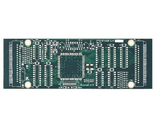
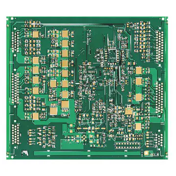
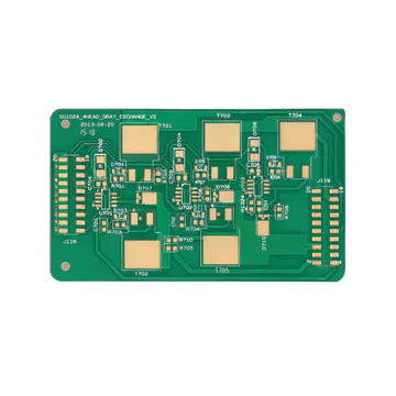
Double Sided Printed Circuit Board Prototyping Polyimide 2-layer Double-layer PCB for Underground detection
Double Layer, Polyimide, 4L/1.6mm
Immersion Gold, ENIG, 12/12mil
Double Layer, Polyimide, 4L/1.6mm
Immersion Gold, ENIG, 12/12mil
SPECIFICATION:
Name: Double-layer PCB
Material: Polyimide
Application: Underground Detection
Layers/plate thickness: 4L/1.6mm
Surface Treatment: ENIG
Line width/line spacing: 12/12mil
Minimum Hole Diameter: 0.50mm
Technical Feature: High Heat resistant material TG250
Two-sided PCB model, the foremost normally surface treatment is HASL. At constant time, OSP, gold plating, immersion gold, immersion silver, is equally applicable.
HASL- sensible appearance, simple to weld tin on the pad, easy welding, low price.
Double sided boards are wide used and relatively easy, each manufacturer can do, that the competition is usually on the price.
ENIG- stable quality, sometimes employed in the case of boding IC. For two sided board, using through hole within the middle connects two-sided traces, and there are 2 more processes than single aspect board, that is Electroless Copper and plating.
Related Products
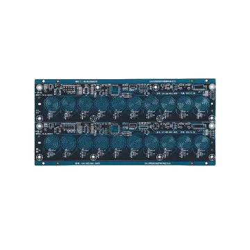
Double Sided Printed Circuit Board Prototyping FR4 2-layer Double-layer PCB for Automation System
Double Sided Printed Circuit Board Prototyping FR4 2-layer Double-layer PCB for Automation System
Double Layer, FR4, 2L/1.6mm
Immersion Gold, ENIG, 10/10mil
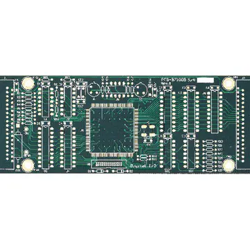
Double Sided Printed Circuit Board Prototyping FR4 2-layer Double-layer PCB
Double Sided Printed Circuit Board Prototyping FR4 2-layer Double-layer PCB
FR4, CEM-1, Rogers;
Immersion Gold, ENIG, Immersion silver/Sn, HASL, LF-HASL, OSP
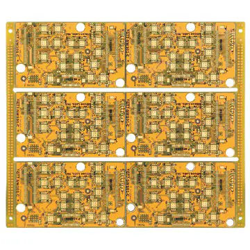
Double Sided Printed Circuit Board Prototyping FR4 2-layer Double-layer PCB for Security
Double Sided Printed Circuit Board Prototyping FR4 2-layer Double-layer PCB for Security
Double Layer, FR4, 4L/1.0mm
Immersion Gold, ENIG, 12/12mil
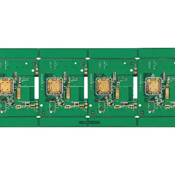
Double Sided Printed Circuit Board Prototyping FR4 2-layer Double-layer PCB for Multimedia Equipment
Double Sided Printed Circuit Board Prototyping FR4 2-layer Double-layer PCB for Multimedia Equipment
Double Layer, FR4, 2L/1.6mm
Gold sinking, ENIG, 4/4mil
Double Sided Printed Circuit Board Copper substrate PCB 2-layer Double-layer PCB for large Printing Equipment
Double Sided Printed Circuit Board Copper substrate PCB 2-layer Double-layer PCB for large Printing Equipment
Double Layer, Copper substrate, 2L/2.0mm
Immersion Gold, ENIG, 10/10mil
Double Sided Printed Circuit Board Prototyping Polyimide 2-layer Double-layer PCB for Underground detection
Double Sided Printed Circuit Board Prototyping Polyimide 2-layer Double-layer PCB for Underground detection
Double Layer, Polyimide, 4L/1.6mm
Immersion Gold, ENIG, 12/12mil